Deprecated: Hook custom_css_loaded is deprecated since version jetpack-13.5! Use WordPress Custom CSS instead. Jetpack no longer supports Custom CSS. Read the WordPress.org documentation to learn how to apply custom styles to your site: https://wordpress.org/documentation/article/styles-overview/#applying-custom-css in /home/u841311238/domains/physicstuff.com/public_html/wp-includes/functions.php on line 6078
Solid State Physics Archives - PhysicStuff

Category: Solid State Physics

What is Graphene?

What is Graphene?

Let’s start with a very short story, two physicists were having fun experimenting and they used scotch tape to remove layers of carbon from a lump of Graphite (material used in pencils). Voila, they made Graphene. And this thing got them the Nobel prize in Physics in 2010. Those two physicists were Andre Geim and Konstantin Novoselov. Now it sounds just too simple but there is still a lot to be known about Graphene.

A lump of graphite, a graphene transistor, and a tape dispenser. Donated to the Nobel Museum in Stockholm by Andre Geim and Konstantin Novoselov in 2010.
Image credits: Wikipedia

Graphene in simple words is a very thin layer of carbon atoms, and by very thin I mean only one atom thick!! It’s a sheet of carbon atoms in hexagonal lattice. Fun fact: When you write with a pencil there’s a chance you might have accidentally created Graphene!

Let’s get straight to the properties of Graphene to help us understand why it is of such significance.

Properties of Graphene:

  • Structure: Graphene is a crystalline allotrope of carbon and is tightly packed in regular hexagonal pattern in one plane.Graphene’s stability is due to its tightly packed carbon atoms and a sp2 orbital hybridisation – a combination of orbitals s, px and py that constitute the σ-bond. The final pz electron makes up the π-bond. These π-bonds are responsible for most of graphene’s notable electronic properties, via the half-filled band that permits free-moving electrons. In simple words sp2 orbital gives graphene its strength and pz electron helps electrons to move easily. It’s actually a perfect 2D structure as its just one atom thick, well in atomic scale its 3D but its the best 2D structure we can get. Something so thin will be obviously very light weight. Apparently less than a gram of graphene sheet can cover an entire football field. And to top it off the structure of Graphene is so strong that it would take an elephant balancing on a sharp pencil to pierce a Graphene sheet with the thickness of Saran Wrap. (This fact about the strength of Graphene sheet is totally mind blowing and hard to digest). In technical terms the tensile strength of Graphene is 130 GPa , for comparison the tensile strength of stainless steel is 860 MPa !!
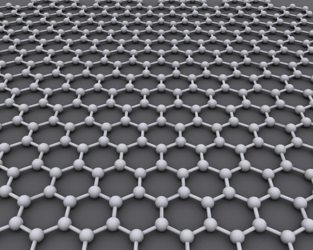
 

Hexagonal structure of Graphene
Hexagonal structure formed by 6 Carbon atoms.
  • Thermal Conductivity: Now we know Graphene is super strong very light weight one atom thick sheet of carbon atoms. As if it wasn’t enough Graphene is better at conducting heat than any other material. It is 10 times better at carrying heat than copper.
  • Electronic Properties: Graphene is also a very very good conductor of electricity. It has very less resistance due to the uniform flat structure of graphene, so the electrons flow very easily. At room temperature it can conduct electricity faster than any other known material.
  • Optical Properties: As Graphene is extremely thin it is almost transparent as one might expect. Infact Graphene transmits about 97% of light which is more than a glass pane.

Summary: So in short Graphene is ultra light, ultra thin, super strong, transparent and a very good conductor of heat and electricity!!

Graphene sheet.
Image credits: www.dailymail.co.uk


Now lets get to the possible applications of this futuristic material.

Applications: 

  • Graphene is transparent and flexible conductor which is very promising for applications in LEDs, Solar cells,  flexible Touchscreens for wearable gadgets, etc.
  • Graphene super-capacitors serve as energy storage alternatives to traditional electrolytic batteries. Some advantages are fast charging, long life span and environment friendly production.
  • According to Moore’s Law, Silicon transistors are becoming smaller and smaller and hence approaching its limits. Graphene can be an exciting replacement in electronic devices due to its amazing properties and many big companies are working on it.
  • Graphene can be used to coat materials to increase their structural strength.
  • Such super materials have a direct application is sports. Like Graphene is used in tennis rackets and is said to have better performance than normal rackets. One other application is in Formula 1 cars (Which is already on a whole another level in terms of engineering and technology) or in sports cars. BAC’s 2016 Mono model is said to be made out of graphene as a first of both a street-legal track car and a production car.
2017 BAC Mono Graphene
Image credits: www.topspeed.com
  • The multifunctional nature of graphene means that it is going to have limitless applications we haven’t even thought of yet. It can be used in aerospace applications, motor vehicles, flexible wearable electronic devices, and many applications in medical and biomedical devices.


Inspite of all these benefits of a material of amazing properties whats stopping us from actually using it in the above applications? Well the method used by Andre Geim and Konstantin Novoselov produces very less amount of Graphene and it may not be a perfect single layer of Graphene. The various methods of Graphene production are Mechanical Exfoliation (which means using scotch tape and other adhesives to peel of layers from Graphite), Chemical Vapour Deposition (in which we can produce comparatively big sheets of Graphene than exfoliation), Dispersing graphite in a liquid medium can produce graphene by sonication followed by centrifugation, etc. But all these methods produce less amounts of Graphene and new methods are being developed to reduce defects and production costs. As Graphene sheets are very difficult to make it is one of the most expensive materials on the planet as of now.

Production and development of Graphene is a very active field of research in the field of material science and it is said to be the material of the future. There might be other materials not yet discovered maybe similar or better than Graphene we don’t know!


How do solar cells work?

How do solar cells work?

The solar cell is an important candidate for an alternative terrestrial energy source because it can convert sunlight directly to electricity with good conversion efficiency, can provide nearly permanent power at low operating cost, and is virtually non-polluting. Solar cell also called as photovoltaic cell and are building blocks of solar panels. You must have seen these panels (large collection of solar cells) in green energy campaigns and also in developed cities in large arrays. It is used as a primary source of energy in space applications. ISS has large solar panels! Let’s understand the basics of solar cells.


The most commonly known solar cell is configured as a large-area p-n junction made from silicon. p-n junctions of silicon solar cells are made by diffusing an n-type dopant into one side of a p-type wafer (or vice versa). To get an idea about p-n junction click here. Now when light or photon hits the p-n junction it dislodges an electron and creates a hole in its place. Now the dislodged electron and hole are free to move in silicon crystal. Due to the electric field present, the electron moves to the n-type region and hole moves to the p-type region. The mobile electrons created in n-type are collected by thin metal fingers on the top of n-type region. Photons having energy equal to the band gap of silicon crystals are the only ones contributing in cells electrical output. Energy greater than band gap is lost as heat. We might also lose energy if electrons and holes recombine as soon as they are formed. So basically a solar cell works by knocking off electron of same energy as band gap of crystal material used and essentially converting light energy into electrical energy.

Schematic representation of silicon p-n junction Solar cell.


The radiative energy output from the sun derives from a nuclear fusion reaction. In every second, about 6 x 10^11 kg hydrogen is converted to helium, with a net mass loss of about 4 x 10^3 kg. We get a lot of energy from sun and if there is a way to harness this energy what’s stopping us from being completely reliant on solar power? There are various factors at play.

Terrestrially the sunlight is attenuated by clouds and by atmospheric scattering and absorption. Also we don’t receive sunlight during night time and during bad weather conditions. This is something we can’t do anything about. As mentioned above, only the photon having energy equal to band gap contributes in electrical output. Photons having energies other than band gap of semiconductor crystals either reflects back or goes through or the energy is just lost as heat energy. Antireflective coating is done to avoid reflection of photons. To deal with photons of energies other than band gap of that semiconductor crystal there is a different approach.

Spectrum Splitting : 

Spectrum splitting is a very good way of increasing efficiency of solar cells by splitting sunlight into narrow wavelength bands and directing each band to a cell that has a band gap optimally chosen to convert just this wavelength band of light. There is one more way, by simply stacking cell on top of one another with the highest band gap cell at the top which automatically achieves an identical spectral-splitting effect, making this “tandem” cell approach a reasonably practical way of increasing cell efficiency.

This is an area of active research where scientists all over the world are trying to increase the efficiency of solar cells. The most efficient solar cell yet still converts only 46% of solar energy into electricity. And most commercial systems convert only 15-20% of solar energy. Solar energy is a source of green and sustainable energy and probably a candidate for future source of energy.

What is p-n junction?

What is p-n junction?

The p-n junctions are elementary building blocks of semiconductor electronic devices. As the name suggest it is a junction between two types of semiconductor materials the p-type and the n-type. The p-type is the positive side of junction and n-type is the negative side. The p-type consists of excess holes (missing electrons) and n-type consists of excess electrons. The junction is the boundary or interface between these 2 types inside a single crystal of semiconductor. When a p-n junction is formed i.e when it is fabricated there are excess electrons on n side and holes on p sides so electrons and holes combine at the junction. Departure of electrons from n side to p side leaves with a positive donor ion on n side and likewise hole leaves negative acceptor ion on p side. The uncompensated ions are positive on n side and negative on p side which creates an electric field which provides a force opposing the continued exchange of charge carriers.

When the electric field is sufficient to stop further transfer of charge carriers the depletion layers reaches an equilibrium. When a positive voltage is applied to the p-side with respect to the n-side, a large current will flow through the junction. However, when a negative voltage is applied, virtually no current flows. This “rectifying” behaviour is the most important characteristic of p-n junction. This is a very short description of p-n junction and how it works.

The p-n junction was invented by Russell Ohl an American physicist of Bell Laboratories in 1939.  The p-n junction is created by doping (adding impurities) by various methods on any one type of base semiconductor material. Various methods like ion implantation, diffusion, etc. Semiconductors for instance silicon, is doped with boron, phosphorus, or arsenic by ion implantation method. In diffusion method the impurity moves into the semiconductor crystal by solid-state diffusion. In the ion-implantation method, the intended impurity is introduced into the semiconductor by accelerating the impurity ions to a high-energy level and then implanting the ions in the semiconductor.

The p-n junction can be used in electronics circuits in two different configurations, forward bias and reverse bias.

In forward bias, the p-type is connected with the positive terminal and the n-type is connected with the negative terminal. With a battery connected this way, the holes in the p-type region and the electrons in the n-type region are pushed toward the junction and start to neutralize the depletion zone, reducing its width. And thus current flows through the junction.Connecting p-type region to the negative terminal of the battery and the n-type region to the positive terminal corresponds to reverse bias. Very little current will flow until the diode breaks down in reverse bias configuration.

The forward-bias and the reverse-bias properties of the p–n junction imply that it can be used as a diode. A p–n junction diode allows electric charges to flow in one direction, but not in the opposite direction; negative charges (electrons) can easily flow through the junction from n to p but not from p to n, and the reverse is true for holes. When the p–n junction is forward-biased, electric charge flows freely due to reduced resistance of the p–n junction. When the p–n junction is reverse-biased, however, the junction barrier (and therefore resistance) becomes greater and charge flow is minimal. p-n junction is used in many semiconductor devices such as diodes, transistors, solar cells, LED’s, integrated circuits, etc.